27 Jul 2018

Facts about North America - North America Map and Globe - Continents of the World

Here are some interesting and very important facts about North America that you should know-


world map, countries of the world, map of the world, USA, Unite states, north america, canada,
World Map (Countries of the World)


North America Facts

1.North America is the third largest continent in the world after Asia and Africa.

2.The total area of North America is 24,709,000 square kilometers (9,540,000 square miles).

3.There are total 23 countries (sovereign States) in the North American continent.

4.Main languages spoken in North America are English, Spanish and French but other languages are also spoken here.

5.United States is the fourth largest country in the world while Canada comes at second position.


North America Map, Map of North America, Globe, world globe, north america globe
North America Map (Globe)

6.Canada and United States of America (USA) together make the Anglo America. 

7.Bering sea and Bering Strait separates the Anglo America from Russia while the Baffin bay and Davis Strait separates it from Greenland. 

8.Florida strait separates the USA from Cuba.

9.Vancouver Island is separated from United States (US) by Juan de fuca Strait.

10.Rio Grande river forms the border between United States and Mexico.

🌓READ THIS ALSO:-
Islands of North America - Interesting Facts about North American Islands that You Never Knew !!!

11.Tropic of Cancer passes through the gulf of Mexico and 49 degree parallel makes boundary between USA and Canada.

12.The largest desert of North America is Sonoran (Mojave) which is in the south California.

13.North America's highest peak is Mt Mckinley which is 6194 meters high while the lowest point is the Death Valley which is 86 meters below the sea level.

14.America is bounded by the Atlantic ocean on the east, the Pacific Ocean on the west, Arctic Ocean on the north,  Caribbean Sea and Panama Canal in the south.

🌓READ THIS ALSO:-
FACTS about EUROPE - MAP of European Countries - European Continent Facts

15.Hoover Dam is on Colorado river which is the highest dam in the world.

16.Main lakes of North America are Superior, Michigan, Huron, Erie and Ontario. All of these lakes except Michigan are shared by USA with Canada. Michigan lake is entirely in the USA.

🌓READ THIS ALSO:-


World Famous Historical Monuments and Landmarks, World Famous Historical Monuments, World Famous Landmarks
World Famous Historical
Monuments and Landmarks


Top Intelligence Agencies
of the World


25 Jul 2018

Universe Origin Theories, Beginning, Evolution and Future of the Universe (BIG BANG Theory, Steady State Theory and Pulsating Theory)

What is the Universe

The universe can be defined as the totality of everything that exists that includes all matter and energy, planets, stars, galaxies and all the content that is present in the intergalactic space.


Origin of The Universe


Theories of Origin and Evolution of the Universe

Here we will discuss, 3 important theories put forward to explain the origin and evolution of the universe -
These theories are -
1. The Big Bang Theory
2. Steady State Theory
3. Pulsating Theory

Now let's discuss each of these theories in some detail-


The Big Bang Theory

The big bang theory was proposed by Le Maitre and Gammow. This theory says that the whole matter of the universe was once concentrated in an extremely dense and hot fireball at the beginning of the universe.
And then very big explosion occurred nearly 20 billion years ago. This big explosion was named "the Big Bang". This big explosion caused the matter to break into pieces. The highly concentrated matter was thrown out with high speed in all the directions that later formed stars and galaxies. These stars and Galaxies are still moving away from each other. Our Universe is expanding !!!


Steady State Theory of Universe

The steady state theory was developed by Bondi, Thomas, Gold German and Fred hoyle. According to this theory,

24 Jul 2018

Current Affairs 23 July 2018 in Hindi/ Daily Current Affairs and News/ करेंट अफेयर्स हिंदी

सीमा सड़क संगठन (BRO) ने भूटान में रणनीतिक रूप से महत्वपूर्ण सड़क का निर्माण पूरा किया

* यह सड़क भूटान के सीमावर्ती शहर फुन-त्सो-लिंग को भूटान की राजधानी थिंपू से जोड़ती है
* इस नई सड़क के निर्माण के बाद भूटान के दक्षिण में स्थित शहर फुन-त्सो-लिंग से राजधानी थिंपू तक की यात्रा का समय लगभग 1 घंटे तक कम हो जाएगा  


अमेरिकी अंतरिक्ष एजेंसी नासा सूर्य के अध्ययन के लिए पार्कर सोलर प्रोब मिशन लॉन्च करेगी

* नासा का यह अति महत्वाकांक्षी मिशन सूर्य का अध्ययन करने के लिए है
* पार्कर सोलर प्रोब मिशन पर नासा द्वारा लगभग 1.5 अरब डॉलर का खर्चा किया जाएगा
* 612 किलो वजन के इस सोलर प्रोब का आकार एक कार के बराबर है
* यह अंतरिक्ष यान 6 अगस्त को रवाना किया जाएगा और सूर्य के बहुत करीब पहुंच कर उसका अध्ययन करेगा
* इस स्पेसक्राफ्ट का नाम अमेरिकी वैज्ञानिक यूजीन न्यूमैन पार्कर  के नाम पर रखा गया है


बिहार सरकार ने सर्वसम्मति से नया शराब संशोधन कानून पारित किया

* बिहार सरकार ने राज्य विधानसभा के मानसून सत्र में शराब निषेध पर एक संशोधन कानून सर्वसम्मति से पारित किया
* 5 अप्रैल 2016 से बिहार में किसी भी प्रकार की शराब पर पूर्ण प्रतिबन्ध लागू किया हुआ है

23 Jul 2018

Modes of Operation of BJT (Active Mode, Cutoff Mode, Saturation Mode, Reverse Active Mode of Transistor)/Bipolar Junction Transistor

Here we will learn the basic concepts of Bipolar Junction Transistor (BJT) and how to operate BJT transistor in different operating modes.

The image shown below shows the schematic symbols for two types of transistors- NPN transistor and PNP transistor


Symbols of NPN and PNP Transistors (BJT)

Symbols of NPN and PNP Transistors, Symbols of BJT Transistors, Representation of NPN and PNP BJT Transistors
Symbols of NPN and PNP BJT Transistors 

In the Image you can easily see that both types of transistors (NPN and PNP Transistors) have 3 terminals- emitter terminal, base terminal and collector terminal.
So why we call these transistor types as NPN or PNP?
Actually the pure form of semiconductor is known as intrinsic semiconductor, but when we add impurities externally in very small amount, then it is called as doping. This doping is done to increase the conductivity of the pure form of semiconductor. The pure form of semiconductor before adding external impurities is called as intrinsic semiconductor but after adding impurities it is known as extrinsic semiconductor.
The extrinsic semiconductors can be of two types- N-Type and P-Type semiconductors.  If electrons are present in majority after doping then it is known as n type of semiconductor but if holes are present in majority then it is called as p type of semiconductor.
So now you can understand that, the NPN transistor contains two N type regions and one P-type region while the PNP transistor contains two P-type regions and one N-type region.

Now see the schematic symbol carefully. Observe the direction of arrow in both types of transistors. In both of these types, the direction of arrow is in P to N direction. The direction of arrow shows the emitter current direction.

The image given below is another representation of BJT transistor
Symbols of NPN and PNP BJT Transistors, NPN and PNP BJT Transistors
Symbolic Representation of NPN and PNP BJT Transistors 

In this image also you can observe the three terminals - emitter, base and collector along with the N and P regions.
In NPN transistor electrons are in majority while holes are in minority but in case of PNP transistor holes are in majority and electrons are in minority.

For transistor to work properly we want that maximum number of electrons or holes (charge carriers) emitted by the emitter region reach to the collector region. 
So because of this the emitter region is doped highest so that it can emit a large number of charge carriers while the base region is doped lightest and its size is made smallest to reduce the recombination of charge carriers (electrons and holes) in the base region.

We can operate the bipolar junction transistor (BJT) in 4 different operating modes.These four modes of operation are-


Operation Modes of Bipolar Junction Transistor (BJT)

*Active mode
*Saturation mode
*Cutoff mode 
*Reverse active mode


Active Mode Operation of BJT Transistor (Bipolar Junction Transistor)

BJT (NPN Transistor) in active mode is shown in the image given below-


 Active Mode Operation of BJT Transistor (Bipolar Junction Transistor),  Active Mode Operation of BJT,  Active Mode Operation of Transistor,  Active Mode Operation of Bipolar Junction Transistor, Active Mode Operation of BJT   Transistor (NPN BJT)
Active Mode Operation of
BJT Transistor(NPN BJT)

In active mode, the emitter-base Junction is forward biased and the collector-base Junction is reverse biased. This mode of operation is also known as active region (forward active region). In active mode the bipolar junction transistor works as an amplifier.
You can see in the image that the emitter base Junction is forward biased. Here we have taken the example of NPN transistor to show the active mode. Observe the emitter and base region - the P-type (base region) is at Higher potential than the N-type (emitter region). Therefore this junction is forward biased. 
But the collector-base junction is reverse biased as N-type region (collector) is at higher potential in comparison to P-type region (base). Now observe this image very carefully. As we know that electrons are majority charge carriers in case of N type semiconductor while holes are in majority in P type semiconductor. As we know that the direction of electric field is from higher potential to lower potential, therefore in this case according to the image, the direction of electric field is from base to emitter at the emitter-base Junction while its direction is from Collector to base at the collector-base Junction.
Since we want, the large amount of charge Carriers that are emitted by the emitter to reach to the collector region. Therefore, the majority charge Carriers (electrons) that are emitted by this N type of emitter, feel force in the direction that is opposite to the direction of electric field (as electrons have negative charge). Therefore the electrons emitted by the emitter are pushed into the base region. Again these electrons experience force towards the collector region because of the direction of electric field (collector to base). Therefore the maximum Number of electrons that are emitted by the emitter reach to the collector region. So this was the operation of NPN transistor in active mode. 
Now we will discuss the same active mode operation in case of PNP transistor. 
Look at the image given below-


Active Mode Operation of PNP BJT, Active Mode Operation of BJT, Active Mode Operation of transistor
Active Mode Operation of PNP BJT

As discussed earlier, The basic condition for active mode operation of the transistor is - the emitter base junction should be forward biased while the collector base junction reverse biased. So in this case of PNP transistor also you can observe the polarities of these two junctions. Here observe the direction of electric field (from higher potential to lower potential). In case of PNP transistor, the emitter emits holes (emitter is of P type having holes as majority charge carriers) and these holes experience force in the direction of electric field as holes are positively charged carriers. Positive charge carriers experience electric force in the direction of the electric field. So as indicated in the diagram, the holes experience force towards base region and reach to the base region from the emitter region. Again these holes feel force towards the collector region when they are in the base region because of the direction of electric field. Hence majority charge carriers (holes) emitted by the emitter (P type) reach to the collector region. So this is also the active mode of operation.


Now let's discuss the cutoff mode of BJT transistor-


Cutoff Mode Operation of BJT (Bipolar Junction Transistor)

In cutoff mode both the junctions of the bipolar junction transistor (emitter-base junction and collector-base Junction) are reverse biased. Because of this, transistor in cut off mode works as an open circuit (OC) switch. It is also called in 'off state' or '0 state'
Look at the image shown here-


 Cutoff Mode Operation of BJT (Bipolar Junction Transistor), Cutoff Mode Operation of BJT (Transistor working as Open Switch),  Cutoff Mode Operation of BJT
Cutoff Mode Operation of BJT (Transistor working as Open Switch)

You can see in this image that no collector current flows (collector current is zero) in the cutoff mode. The image also shows another representation of the cut off mode. This image shows the symbol of an open circuit as no current flows through an open circuit. 

Note-The transistor acts as a switch (open switch) in the cutoff mode. The image given below depicts the cutoff mode. You can observe here that both junctions are reverse biased. This image also indicates the direction of electric field.


 Cutoff Mode Operation of BJT (Bipolar Junction Transistor),  Cutoff Mode Operation of BJT,  Cutoff Mode Operation of Bipolar Junction Transistor
Cut off Mode Operation of BJT
(Bipolar Junction Transistor)

Now we will discuss the saturation mode.


Saturation Mode Operation of BJT (Bipolar Junction Transistor)

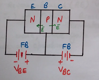
The image given below shows the BJT transistor in saturation mode. In saturation mode of the transistor, both the junctions (emitter-base junction and collector-base Junction) are forward biased. You can also observe this biasing in this image. The direction of electric field is also depicted in the diagram.

 Saturation Mode Operation of BJT (Bipolar Junction Transistor),  Saturation Mode Operation of BJT,  Saturation Mode Operation of Bipolar Junction Transistor
Saturation Mode Operation of BJT
(Bipolar Junction Transistor)

The another image given below shows- that in saturation mode, the transistor acts as a Switch (Closed Switch) or short circuit. As clear by the image that in saturation mode maximum collector current flows. The transistor in saturation mode is also said to be in '1 state' or 'ON state'


Saturation Mode Operation of BJT (Transistor working as a Closed Switch), Saturation Mode Operation of BJT, Saturation Mode Operation of Transistor working as a Closed Switch
Saturation Mode Operation of BJT
(Transistor working as a Closed Switch)

In saturation mode the transistor can be under one of the two modes-
#Forward saturation region
#Reverse saturation region

If the Emitter junction voltage > collector junction voltage
Then the transistor is called under forward saturation region

But if collector junction voltage > emitter junction voltage
Then the transistor is under reverse saturation region.

Now we will discuss the reverse active mode


Reverse Active Mode Operation of BJT (Bipolar Junction Transistor)

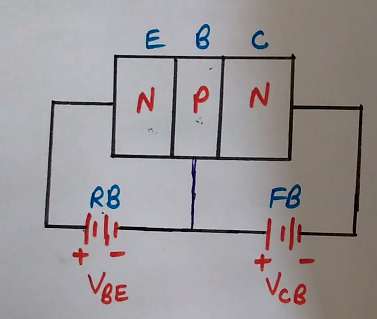
The reverse active mode is just opposite to the active mode because in this mode of operation the emitter-base junction is reverse biased while the collector-base junction is forward biased.
As the gain is negligible in this mode of operation, therefore the transistors in never operated in reverse active mode. Because it is just opposite to the transistor action that we desire.
To understand the reverse active mode you can see this image-
Reverse Active Mode Operation of BJT
(Bipolar Junction Transistor)

This image clearly shows that the emitter-base junction is reverse biased and the collector-base junction is forward biased. This biasing of junctions is exactly opposite to the active mode of operation of the transistor. Therefore this mode of operation is called as reverse active mode.
So this was all about different types of operating modes of Bipolar Junction Transistor (BJT).

Read More-

Go To HOME Page
   
FREQUENCY SPECTRUM OF AMPLITUDE MODULATION (WAVEFORMS AND EQUATIONS DERIVATION)

AMPLITUDE MODULATION (TIME DOMAIN EQUATIONS AND WAVEFORMS)

ADVANTAGES AND DISADVANTAGES OF DIGITAL COMMUNICATION SYSTEM

ADVANTAGES OF OPTICAL FIBER COMMUNICATION

STEP INDEX OPTICAL FIBER (MULTIMODE AND SINGLE MODE STEP INDEX FIBERS)

PULSE MODULATION TECHNIQUES (PAM, PWM, PPM, PCM)

OPTICAL FIBER: STRUCTURE AND WORKING PRINCIPLE

PULSE AMPLITUDE MODULATION (PAM)

COMPARISON OF PAM, PWM, PPM MODULATION TECHNIQUES

PULSE WIDTH MODULATION (PWM)

CONTINUOUS TIME AND DISCRETE TIME SIGNALS (C.T. AND D.T. SIGNALS)

NEED AND BENEFITS OF MODULATION

PULSE POSITION MODULATION (PPM)

OPTICAL FIBERS IN COMMUNICATION: COVERS ALL IMPORTANT POINTS

OPTICAL FIBER SOURCES (DESIRABLE PROPERTIES)

AMPLITUDE MODULATION Vs FREQUENCY MODULATION (ADVANTAGES AND DISADVANTAGES)

PULSE CODE MODULATION (PCM) [ADVANTAGES AND DISADVANTAGES]

SAMPLING THEOREM AND RECONSTRUCTION (SAMPLING AND QUANTIZATION)

SUPERPOSITION THEOREM (BASICS, SOLVED PROBLEMS, APPLICATIONS AND LIMITATIONS)

Digital Modulation Techniques (ASK, FSK, PSK, BPSK)/ Amplitude, Frequency and Phase Shift Keying

Conventional AM Vs DSB-SC Vs SSB-SC Vs VSB (Comparison of AM Systems)

Quadrature Amplitude Modulation (QAM)/ QAM Transmitter and QAM Receiver Block Diagram

Single-Mode Optical Fiber Advantages

What are Microwaves and their Applications (Uses) in various fields

Microwaves Properties and Advantages (Benefits)

Basic Structure of Bipolar Junction Transistor (BJT) - BJT Transistor - Working and Properties

Polar Plots of Transfer Functions in Control Systems (How to Draw Nyquist Plot Examples)

Generation of Binary Phase Shift Keying (BPSK Generation) - Block Diagram of Binary Phase Shift Keying (BPSK)

Low Level and High Level Modulation Block Diagram (AM Transmitter Block Diagram)

Block Diagram of CRO (Cathode Ray Oscilloscope), Components of CRO and CRT with Structure and Working

Slope Overload Distortion and Granular (Idle Noise), Quantization Noise in Delta Modulation

Frequency Translation/Frequency Mixing/Frequency Conversion/Heterodyning (Basic Concepts and Need)

Quadrature Phase Shift Keying Modulation (QPSK) Basics, Waveform and Benefits

Pulse Code Modulation (PCM) Vs Differential Pulse Code Modulation (DPCM)


17 Jul 2018

Basic Structure of Bipolar Junction Transistor (BJT) - BJT Transistor - Working and Properties

In this post we will discuss the Bipolar Junction Transistor (BJT). The basic structure of BJT and its various properties will be explained here in detail.


Structure of Bipolar Junction Transistor (BJT)

The diagram shown below is the basic structure of Bipolar Junction Transistor-


Structure of Bipolar Junction Transistor (BJT), construction of Bipolar Junction Transistor (BJT), structure of bjt transistor
Structure of Bipolar Junction Transistor (BJT)

The reason behind why it is known as bipolar junction transistor is; it has two types of charge carriers- electrons and holes. These electrons or holes may be present in majority or minority in BJT.


Watch the Complete Video Here


While in case of Field Effect Transistors (FETs) and Metal Oxide Semiconductor Field Effect Transistors (MOSFETs), we have only one type of charge carriers in majority, either electrons or holes. Minority charge carriers are not present in FETs or MOSFETs. Therefore FETs and  MOSFETs are known as unipolar devices.
You can easily see the emitter region, base region and the collector region in the diagram of bipolar junction transistor shown above. These three regions form two junctions.
The junction formed by emitter and base regions is known as emitter-base Junction or emitter junction while the base and collector regions form the collector-base Junction (collector Junction).

12 Jul 2018

Polar Plots of Transfer Functions in Control Systems (How to Draw Nyquist Plot Examples)

In this post we will learn what are polar plots. Here we will also trace polar plots of some transfer functions also.
Here we will see the general shapes of the polar plots of some important transfer functions. You will learn in this post, how the shape of the polar plot changes on adding poles (non zero poles and poles at origin) or zeros to the transfer function.
But before this it is important to understand what we mean by polar plots-

Watch the Complete Video Here-

What is Polar Plot in Control System

A polar plot is a plot of a function that is expressed in polar coordinates, with radius as a function of angle.
Polar plots are drawn between magnitude and phase.
If we have a sinusoidal transfer function G(jw), which is a complex function.
Therefore we can write-
G(jw)= Re[G(jw)] + jIm[G(jw)]
G(jw)= lG(jw)l angle(G(jw))

Therefore we can represent the transfer function G(jw), as a phasor of magnitude M and phase angle phi. This phase angle is measured positively in the counter clockwise direction.
The magnitude and the phase angle changes as the input frequency (w), is varied from zero to infinity.
So the locus obtained in the complex plane by the tip of the phasor G(jw) is called the polar plot.
Polar plots are also known as a Nyquist Plots.

Now we will understand the effect on shape of the polar plot on adding poles or zeros to the transfer function.


Polar Plots of Transfer Functions (Adding Poles and Zeros)

There are following three rules that are followed to trace Polar Plots in control systems, on adding poles and zeros to the transfer function-

Generation of Binary Phase Shift Keying (BPSK Generation) - Block Diagram of Binary Phase Shift Keying (BPSK)

Here we will understand the generation of BPSK signal. BPSK stands for Binary Phase Shift Keying. With the help of block diagram we will discuss the concept of Binary Phase Shift Keying generation.
But before discussing the generation of Binary Phase Shift Keying, we will first understand what is Phase Shift Keying (PSK).


Watch the Complete Video Here-

Phase Shift Keying (PSK) Introduction

In Phase Shift Keying, the phase of the carrier wave (analog) is switched as per the input digital signal. This is analogous to Phase Modulation (PM).
As we know, in case of phase modulation, phase of the carrier wave is changed according to the instantaneous value of the modulating signal. In the same way, in phase shift keying also, the phase of the sinusoidal carrier wave is changed according to the digital input signal. So the basic difference between analogue modulation and digital modulation is based on the nature of the modulating signal (message signal).

6 Jul 2018

GRE Syllabus 2018-2019- GRE Exam Pattern and Syllabus 2018 (Graduate Record Examinations Syllabus 2018-2019)

Graduate Record Examinations (GRE) is a standardized test, that is conducted by Educational testing Services (ETS). GRE score is accepted by most of the Graduate Schools in the Unites States for the Masters Programs.


GRE Syllabus and Exam Pattern 2018-2019
Following are the 3 main segments of the GRE syllabus:-


Verbal Reasoning:

The verbal reasoning section has following 
3 types of questions- 
*Reading Comprehension
*Text Completion
*Sentence Equivalence